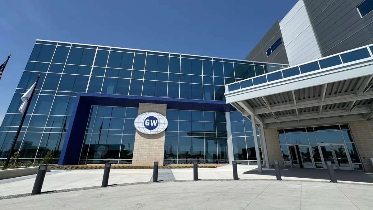
GlobalWafers Co. plans to spend an additional $4 billion on its U.S. manufacturing operations, the semiconductor maker announced Thursday at its 300mm silicon wafer manufacturing facility opening in Sherman, Texas.
The funding includes growing its 142-acre Sherman campus, which provides space for the Taiwan-based company to increase capacity and keep up with other chip producers that have recently announced over $1 trillion in U.S. investments, such as IBM, TSMC, Apple and Nvidia.
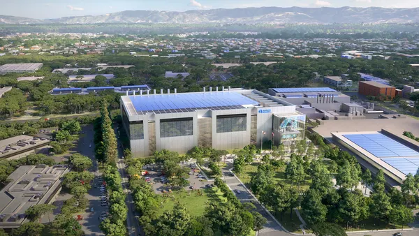
The Sherman facility’s initial investment was $3.5 billion, and will serve as the flagship for GlobalWafers America. The site is also the company’s largest silicon wafer facility, according to its website. As of Friday, the Sherman project created 1,200 construction and 180 permanent jobs, with plans to hire up to 650 engineering, technical and operational employees by the end of 2028, the company said in the release.
The GlobalWafers’ Texas facility is also a recipient of $406 million through CHIPS and Science Act funding. The company is one of the lucky few to inalize its funding contract before former President Joe Biden left the White House.
The money will also go toward GlobalWafers’ other U.S. facility in St. Peters, Missouri, operated through its subsidiary MEMC, which will produce 300mm silicon-on-insulator wafers.
The 300mm wafers are critical for making semiconductors used in home appliances, automobiles, computers, cell phones and artificial intelligence technologies. The polished and epitaxial wafers eliminate surface contamination and improve the electronic devices’ performance.