Dive Brief:
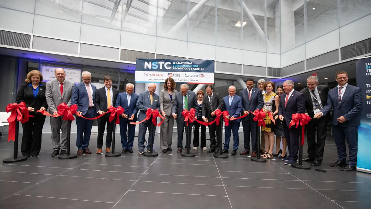
- The Commerce Department opened a CHIPS and Science Act-funded National Semiconductor Technology Center, a research and development flagship facility in Albany, New York, on Monday.
- The CHIPS for America Extreme Ultraviolet Accelerator will provide dedicated space and resources to enhance EUV technology and scale up chip manufacturing, according to the press release.
- The facility is located in the R&D hub NY Creates’ Albany NanoTech Complex and is run by the Commerce Department’s nonprofit, Natcast. Operations officially began July 1.
Dive Insight:
The National Semiconductor Technology Center is a key component of the CHIPS Act and a consortium focused on semiconductor R&D in the United States.
The initiative has a membership program that involves industry, academic and government stakeholders collaborating in the semiconductor R&D space as well as fostering workforce development programs. Members include Google, Apple, TSMC, Nvidia, Intel, Texas Instruments, IBM, Massachusetts Institute of Technology, Arizona State University and Purdue University, according to Natcast’s website.
The EUV Accelerator site will provide collaborators access to lithography tools and R&D capabilities, including a standard high-numerical-aperture EUV machine.
The high NA EUV system, produced by Netherlands-based ASML, uses light with a wavelength of 13.5 nanometers to provide higher contrast and print microchips with an 8 nm resolution, according to the company’s website. The machine enables semiconductor makers to pattern the finest details on advanced microchips.
New York officials have been working to increase its semiconductor presence. The state forged a $10 billion partnership with semiconductor giants such as IBM, Micron and Applied Materials to establish the EUV Accelerator at the Albany Nanotech Complex in December 2023.
The state is also investing $1 billion to expand Albany’s nanotech campus, as well as purchase ASML’s next-generation high NA EUV machine, which is scheduled for release in 2026.
The funds will also be allocated toward the construction of the NanoFab Reflection, Gov. Kathy Hochul said in a July 14 press release. The building will feature more than 50,000 square feet of cleanroom space to support future partner growth and initiatives, including the NSTC, the National Advanced Packaging Manufacturing Program, and the Department of Defense’s Microelectronics Commons program. The project is expected to take two years to complete and will create approximately 500 to 600 union construction jobs.
The state’s partnership with the semiconductor companies led to the Commerce Department choosing Albany as the first CHIPS for America R&D flagship in October 2024, Hochul added. Additionally, the EUV Accelerator is set to receive a proposed federal investment of $825 million.
Hochul also signed legislation into law to draw semiconductor titans to invest and expand in New York. In August 2022, the state passed the Green CHIPS law to help reduce construction costs and operation costs for chip fabs through expanded tax credits. Earlier this year, companies such as Micron and IBM, which have existing facilities in the state, committed $200 billion and $150 billion, respectively, to expand their U.S. manufacturing and R&D footprint.
The EUV Accelerator is one of three NSTC facilities in the United States. The Commerce Department designated Sunnyvale, California, in November 2024 as the second semiconductor R&D hub, which will focus on chip design, electronic design automation, architecture and security.
In January, the Commerce Department chose Arizona State University Research Park in Tempe, Arizona, as the third semiconductor R&D flagship. The facility will focus on prototyping and packaging, featuring advanced 300-millimeter wafer capabilities.